

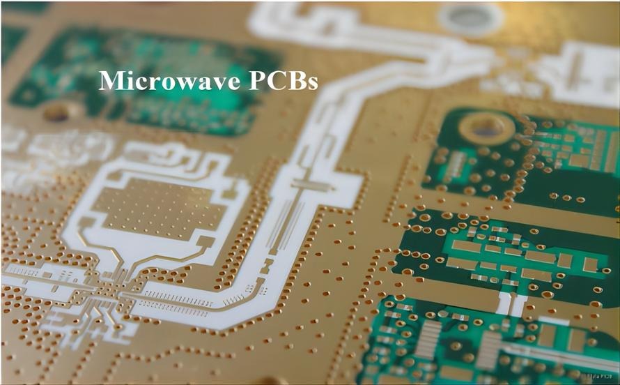
The demand for smaller, faster, and more powerful electronic devices has transformed the way printed circuit boards are designed and manufactured. Modern products such as smartphones, wearable devices, medical equipment, automotive electronics, artificial intelligence hardware, and 5G communication systems require circuit boards capable of supporting extremely high component density while maintaining outstanding electrical performance. Traditional PCB manufacturing methods often struggle to meet these requirements because conventional through-hole vias consume valuable routing space and limit circuit complexity. This challenge has led to the widespread adoption of the Microvia PCB, an advanced circuit board technology that enables compact, high-performance electronic designs.
Microvias are laser-drilled holes with significantly smaller diameters than conventional mechanically drilled vias. They create electrical connections between adjacent PCB layers without passing through the entire board thickness, allowing engineers to maximize routing density while improving signal integrity and reducing board size. As electronic devices continue to evolve toward greater miniaturization, microvia technology has become a critical component of High-Density Interconnect (HDI) PCB manufacturing.
Producing reliable microvia circuit boards requires specialized equipment, precision engineering, and strict process control. For this reason, businesses increasingly collaborate with an experienced Microvia PCB manufacturer that can consistently deliver high-quality boards for demanding applications.
This article explores microvia PCB technology, its manufacturing process, advantages, applications, and the importance of selecting the right manufacturing partner.
What Is a Microvia PCB?
A Microvia PCB is a printed circuit board that uses laser-drilled microvias instead of traditional mechanically drilled holes to create electrical connections between circuit layers. A microvia typically has a diameter of less than 150 micrometers, making it significantly smaller than conventional vias used in standard PCB fabrication.
Unlike through-hole vias that extend across the entire thickness of the board, microvias generally connect only adjacent layers. This design preserves routing space on internal layers and allows engineers to accommodate more electrical connections within a compact PCB layout.
Microvias are a defining feature of High-Density Interconnect (HDI) technology and are commonly combined with fine-line circuitry, sequential lamination, and multilayer construction to support increasingly sophisticated electronic products.
By enabling higher circuit density and improved electrical performance, microvia PCBs have become essential for many advanced electronic applications.
Why Microvia Technology Is Important
As semiconductor packages become smaller and electronic products integrate more functions into limited space, circuit board designers face increasing challenges related to routing density and signal performance. Conventional through-hole vias occupy valuable board space and often restrict the placement of components beneath advanced integrated circuit packages.
Microvia technology addresses these limitations by creating extremely small interconnections that require minimal board area. This allows designers to place components closer together while increasing the number of available routing channels.
The shorter electrical pathways provided by microvias also improve signal integrity by reducing transmission delays, minimizing parasitic capacitance, and lowering electromagnetic interference. These characteristics become increasingly important in high-speed digital circuits operating at gigahertz frequencies.
Additionally, smaller via structures improve thermal performance by allowing more efficient layer design and power distribution throughout the PCB.
These advantages make microvia technology an essential solution for modern high-performance electronic systems.
The Microvia PCB Manufacturing Process
Manufacturing a microvia PCB involves highly specialized fabrication techniques that require exceptional precision. The process begins after engineers finalize the PCB design and define the layer stack-up, via structures, and routing requirements.
Before production starts, manufacturers perform a detailed Design for Manufacturability (DFM) review to evaluate trace widths, via dimensions, copper balancing, layer alignment, and fabrication tolerances. This engineering analysis helps optimize production while improving long-term reliability.
Unlike traditional vias that are created using mechanical drilling, microvias are produced using laser drilling systems capable of generating extremely small and highly accurate holes. Laser technology provides excellent positional accuracy while minimizing damage to surrounding materials.
After drilling, the microvias undergo copper plating to establish reliable electrical connections between adjacent layers. Multiple sequential lamination cycles may be required depending on the complexity of the PCB structure and the number of stacked or staggered microvias included in the design.
The remaining fabrication process includes circuit imaging, chemical etching, solder mask application, surface finishing, silkscreen printing, and final inspection before the completed boards undergo electrical testing and shipment.
Throughout production, manufacturers maintain strict process control because even microscopic dimensional variations can significantly influence product performance.
Advantages of Microvia PCB Technology
Microvia PCBs provide several important advantages that support the development of today’s advanced electronic products. One of the most significant benefits is increased routing density. Smaller vias occupy less board space, allowing engineers to design compact multilayer circuit boards capable of supporting complex semiconductor packages.
Improved signal integrity is another major advantage. Because microvias create shorter electrical pathways between layers, they reduce signal delay, impedance discontinuities, and electromagnetic interference, making them ideal for high-speed digital and radio-frequency applications.
Microvia structures also contribute to better thermal performance by enabling more efficient layer utilization and optimized heat distribution throughout the PCB. This helps maintain stable operating temperatures for high-performance processors and power devices.
Mechanical reliability is enhanced because laser-drilled microvias experience lower mechanical stress compared to larger mechanically drilled holes. Properly manufactured microvias provide excellent long-term durability under demanding operating conditions.
Although microvia fabrication requires advanced manufacturing technology, the resulting improvements in miniaturization, electrical performance, and reliability make this technology highly valuable for modern electronics.
Applications of Microvia PCBs
Microvia PCBs are widely used across industries requiring compact size, high-speed performance, and exceptional reliability. Consumer electronics manufacturers utilize microvia technology in smartphones, tablets, laptops, gaming devices, wearable electronics, digital cameras, and foldable devices where board space is extremely limited.
Telecommunications equipment supporting 5G infrastructure relies on microvia PCBs to achieve high-frequency signal performance while accommodating increasingly complex integrated circuits.
Automotive manufacturers use microvia technology in advanced driver assistance systems, electric vehicle battery management systems, autonomous driving platforms, infotainment units, radar modules, and electronic control systems requiring compact and reliable circuit designs.
Medical device manufacturers depend on microvia PCBs for diagnostic imaging equipment, portable healthcare devices, implantable electronics, patient monitoring systems, and surgical instruments where miniaturization and long-term reliability are essential.
Industrial automation systems, robotics, aerospace electronics, defense equipment, artificial intelligence hardware, cloud computing servers, and Internet of Things (IoT) devices further demonstrate the versatility of microvia PCB technology.
Why Choosing an Experienced Microvia PCB Manufacturer Matters
Producing reliable microvia PCBs requires specialized expertise that extends beyond conventional PCB fabrication. An experienced Microvia PCB manufacturer understands the challenges associated with laser drilling, sequential lamination, copper plating, controlled impedance, and high-density circuit design.
Professional manufacturers provide valuable engineering support during product development by conducting comprehensive Design for Manufacturability reviews. These evaluations optimize via placement, layer stack-up, trace geometry, and manufacturing tolerances before production begins.
Advanced manufacturing facilities equipped with laser drilling systems, automated optical inspection equipment, high-precision plating technology, intelligent manufacturing platforms, and sophisticated process monitoring enable manufacturers to consistently produce high-quality microvia structures.
Working with an experienced manufacturer also ensures greater production consistency, shorter development cycles, and improved long-term reliability across both prototype and high-volume manufacturing.
Quality Assurance in Microvia PCB Manufacturing
Quality control is especially important in microvia PCB production because the extremely small dimensions leave little tolerance for manufacturing defects. Every production stage requires careful inspection to verify dimensional accuracy and electrical performance.
Manufacturers begin by inspecting incoming materials before monitoring laser drilling accuracy, copper plating thickness, layer alignment, and via integrity throughout fabrication.
Automated Optical Inspection (AOI) identifies surface defects while X-ray inspection evaluates hidden microvias, multilayer structures, and internal copper connections that cannot be examined visually.
Electrical testing confirms circuit continuity and insulation resistance, while controlled impedance verification ensures signal transmission meets design specifications. Many manufacturers also perform thermal cycling, vibration testing, humidity testing, and reliability analysis depending on customer requirements.
Leading manufacturers maintain internationally recognized certifications including ISO 9001, IPC standards, UL certification, IATF 16949 for automotive electronics, ISO 13485 for medical devices, and RoHS compliance, demonstrating their commitment to producing reliable high-performance circuit boards.
Future Trends in Microvia PCB Technology
As electronic devices continue becoming more compact and powerful, microvia technology will play an increasingly important role in future PCB development. Artificial intelligence, autonomous vehicles, cloud computing, wearable healthcare devices, 6G communication networks, advanced robotics, and semiconductor innovation will continue driving demand for higher circuit density.
Manufacturers are investing in finer laser drilling capabilities, stacked microvia technologies, ultra-high-density interconnect architectures, advanced substrate materials, and intelligent factory automation to support future electronic products.
The continued development of chiplet architectures, advanced semiconductor packaging, and heterogeneous integration will require even more sophisticated microvia designs capable of supporting unprecedented levels of electrical complexity.
Artificial intelligence-driven manufacturing systems, automated inspection technologies, and precision process control will further improve manufacturing quality while enabling the next generation of high-density electronic products.
Conclusion
The Microvia PCB has become an essential technology for modern electronics by enabling greater circuit density, improved signal integrity, enhanced thermal performance, and significant product miniaturization. Its laser-drilled interconnection structures support increasingly sophisticated semiconductor packages while allowing engineers to design compact, reliable, and high-performance electronic systems.
Choosing an experienced Microvia PCB manufacturer provides access to specialized engineering expertise, advanced fabrication technologies, comprehensive quality assurance, and reliable production capabilities. As electronic products continue to evolve toward higher speeds, smaller form factors, and greater functionality, microvia PCB technology will remain a critical foundation for innovation across consumer electronics, automotive systems, telecommunications, medical devices, aerospace, and countless other high-tech industries.
