

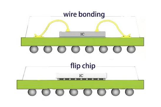
On paper, two optical PCBA quotes can look alike. One says die attach. The other says wire bonding. For the package engineer, the difference is hard to miss. The flip joint is buried under the die. The wire-bond loop is up in the air, where the lid, probe, or repair tool might meet it. That one choice can change the cap clearance, heat route, probe access, and repair plan.
SUNWIN’s precision optoelectronic packaging page covers die attach, wire bonding, optical alignment, and inspection. It is useful when building a supplier shortlist. The released drawing, approved materials, and customer limits still control the job.
Flip-Chip Assembly vs wire bonding for optical PCBA: what is the difference?
With flip-chip, the die is turned over and its bumps or pads land on the substrate. With wire bonding, the die stays face up and fine wires run to the package pads. The useful question is less about the name and more about the finished package: can the team inspect it, cool it, test it, and service it without moving the optical datum?
Decision point
Flip-Chip Assembly
Wire bonding
Connection
Bumps or pads below the die
Fine wires from die to pads
Space question
Is there enough access to inspect the hidden joint?
Will the loop clear the lid and optical path?
Useful record
Placement, joint coverage, void and electrical data
Bond image, pull or shear and electrical data
SUNWIN also lists die attach and gold wire bonding. I would ask the supplier to show the checks for this die finish and substrate, rather than hand over a generic process sheet.
When should an OEM choose each option in Flip-Chip Assembly vs wire bonding for optical PCBA?
Start with the package drawing. A low-profile receiver with a short electrical path may suit Flip-Chip Assembly, provided the bump, substrate, and heating cycle are qualified. A design that needs a visible pad, a test probe, or regular repair may suit wire bonding. If alignment or sealing dominates the risk, compare the whole stack. The interconnect is only one part of that decision.
I would put four questions on the RFQ: Where is the optical datum? How much lid clearance remains? How will the joint be inspected? Who can authorize rework? Those questions usually narrow the choice faster than a price comparison.
Flip-Chip Assembly vs wire bonding for optical PCBA: process, quality and cost trade-offs
The beginning of the traveler may look familiar in both cases: incoming inspection, placement, cleaning, final electrical checks. Then the routes split. Flip-chip needs bump and pad checks, controlled placement, joint or underfill evidence, and a way to inspect a connection that is no longer visible. Wire bonding needs a bond program, capillary control, loop inspection, and a pull or shear sample.
SUNWIN’s optical transceiver PCBA information references inspection and traceability. In a quote, I would separate assembly, fixtures, programming, qualification samples, customer tests, and rework. Otherwise the cheaper quote may just have more exclusions.
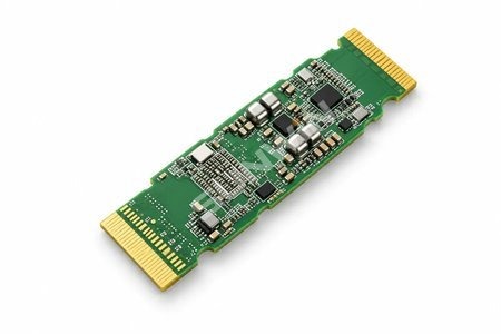
Optical transceiver PCBA die attach and bonding work at SUNWIN.
Flip-Chip Assembly vs wire bonding for optical PCBA: reliability and thermal-management differences
Ask what failure would look like in the finished package. For the face-down route, I would look at placement, coverage or voids, substrate bow, heat-spreader contact, and the cycling behind the qualification. For the wire route, I would want pull data, wire sweep, heel condition, loop clearance, and the expansion mismatch among die, wire, and package.
Do not leave the thermal result by itself. Put the sample, fixture, measurement point, and temperature beside it. A short electrical route is not proof of a good heat route. A tidy loop is not proof that a lid will stay clear after closure.
Supplier qualification checklist for Flip-Chip Assembly vs wire bonding for optical PCBA
Pick one serialised unit. Follow it backwards: die lot, substrate lot, attach material, program revision, inspection image, pull or shear result, rework decision, final test. Can the supplier retrieve the chain without asking an operator to reconstruct the story from memory?
SUNWIN’s quality management system describes traceability and inspection controls. Request a redacted lot record and look for the drawing revision, material batch, equipment ID, and disposition. A capability slide tells you what a line can do. The record tells you what happened to the unit in front of you.
What should an RFQ specify for Flip-Chip Assembly vs wire bonding for optical PCBA?
Send the die dimensions, pad or bump finish, substrate finish, optical axis, bond map, alignment tolerance, thermal interface, material rules, inspection limits, drawing revision, sample count, forecast, fixture owner, and change authority. Write beside the price what it covers: materials, development, alignment, and finished-package testing.
If Full Turnkey Manufacturing is requested, name the customer-supplied chips, allowed substitutes, and the person who can approve a change. Only then do two quotes mean the same thing.
Flip-Chip Assembly vs wire bonding for optical PCBA with Die Attach and Gold Wire Bonding: manufacturing considerations
Write the route as a handoff list people can sign. A flip traveler may start at die preparation and finish at placement, underfill, inspection, and optical or electrical validation. The wire traveler adds die attach, cure, bond programming, pull sampling, cleaning, and closure.
On a mixed transceiver, mark the devices that use Flip-Chip Assembly and the ones that use Die Attach and Gold Wire Bonding. Put the datum, bond map, thermal path, test, sample plan, and retention rule beside each device. SUNWIN’s manufacturing and quality scope can be compared with the same file set. Do not read yield or lead time into a machine name.
Die Attach and Gold Wire Bonding and Optical Transceiver PCBA requirements for Flip-Chip Assembly vs wire bonding for optical PCBA
The RFQ should say what releases each device. If a bad joint can be repaired, name the authority and the closing record. If it cannot, define quarantine and disposition before the first lot. That small decision prevents a late argument over whether a visually good unit is releasable.
FAQs
Q: Is Flip-Chip Assembly always better for high-speed optical devices?
A: No. It can shorten an interconnect and lower the package, but the finished unit still has to meet alignment, thermal, inspection, material, and reliability limits. Wire bonding may fit better when the team needs visible joints or probe access.
Q: What evidence should an OEM request for wire-bonded optical PCBA?
A: Ask for the bond map, program revision, bond images, pull or shear method, sampling rule, nonconformance records, and final optical and electrical results. Each record should identify its lot, materials, equipment, and acceptance limit.
Q: Can SUNWIN quote both Flip-Chip Assembly and wire bonding?
A: SUNWIN can review the package and discuss die attach, bonding, inspection, and test scope. Send the current drawing, BOM, package stack, sample plan, and limits. The quote can then show the included materials, fixtures, alignment work, and tests.
