
The telecommunications industry is the backbone of global connectivity, enabling voice communication, internet access, data transmission, cloud computing, and emerging technologies such as 5G and the Internet of Things (IoT). Behind every telecom device and network infrastructure component lies a sophisticated electronic system built on printed circuit boards. These circuit boards are responsible for processing signals, managing data, and ensuring reliable communication across vast distances. As telecom equipment becomes more advanced, the importance of telecom PCB assembly continues to grow.
Telecom PCB assembly involves the manufacturing and integration of electronic components onto printed circuit boards specifically designed for telecommunications applications. These assemblies must deliver exceptional reliability, high-speed signal performance, and long-term durability because communication networks operate continuously and often under demanding environmental conditions. Understanding telecom PCB assembly is essential for businesses, engineers, and product developers involved in modern communication technology.
What Is Telecom PCB Assembly?
Telecom PCB assembly is the process of assembling electronic components onto printed circuit boards used in telecommunications equipment. These boards serve as the foundation for devices that transmit, receive, process, and manage communication signals across wired and wireless networks.
The assembly process includes mounting components such as microprocessors, communication chips, amplifiers, filters, antennas, connectors, power management devices, and memory modules onto a fabricated PCB. Once assembled, the board becomes a functional electronic system capable of supporting complex communication functions.
Unlike standard consumer electronics, telecom assemblies often require higher levels of performance, reliability, and signal integrity. Communication equipment must handle large volumes of data while maintaining stable operation over extended periods. As a result, telecom PCB assembly requires advanced manufacturing processes and strict quality control standards.
Why Telecom PCB Assembly Is Important
Modern communication systems rely on highly reliable electronic hardware to maintain uninterrupted connectivity. Whether supporting cellular networks, fiber-optic infrastructure, satellite communications, or enterprise networking equipment, telecom PCBs play a critical role in enabling data transmission and signal processing.
A single assembly defect can affect network performance, cause communication failures, or lead to costly service disruptions. Therefore, telecom PCB assembly must meet rigorous manufacturing and testing requirements to ensure dependable operation.
In addition to reliability, telecom equipment often requires high-speed data processing capabilities. Advanced PCB assemblies support these requirements through precise component placement, controlled impedance routing, and optimized signal pathways.
As communication networks continue to expand and evolve, high-quality telecom PCB assembly remains essential for maintaining network efficiency and performance.
Applications of Telecom PCB Assembly
Telecom PCB assembly is used in a wide range of communication devices and infrastructure systems. Cellular base stations represent one of the most important applications. These systems enable wireless communication by transmitting and receiving signals between mobile devices and network operators.
Network routers and switches also depend on advanced PCB assemblies to manage internet traffic and data routing. These devices process enormous volumes of information while maintaining low latency and high reliability.
Fiber-optic communication systems utilize telecom PCBs to support signal conversion, transmission control, and network management functions. Satellite communication equipment similarly relies on specialized assemblies capable of operating in demanding environments.
Additional applications include wireless communication modules, radio frequency systems, broadband infrastructure, data centers, cloud networking hardware, and emerging 5G technologies.
The widespread use of telecom PCB assembly demonstrates its importance in modern communication ecosystems.
Key Features of Telecom PCB Assemblies
Telecommunications equipment requires circuit boards with characteristics that support high-performance operation. One of the most important features is signal integrity. High-speed communication systems must minimize signal loss, interference, and transmission errors.
To achieve this, telecom PCBs often incorporate controlled impedance designs, multilayer board structures, and advanced routing techniques. These features help maintain signal quality throughout the communication process.
Reliability is another critical requirement. Telecom equipment frequently operates around the clock, making long-term durability essential. Manufacturers use high-quality materials and stringent assembly processes to ensure dependable performance.
Thermal management also plays an important role. Communication systems generate significant heat during operation, requiring effective cooling solutions and optimized board layouts to maintain stable performance.
These characteristics distinguish telecom PCB assemblies from many other types of electronic products.
The Telecom PCB Assembly Process
The telecom PCB assembly process begins with reviewing engineering documentation, including Gerber files, bills of materials, assembly drawings, and performance specifications. Careful planning ensures that the assembly process meets the technical requirements of the final product.
Solder paste is applied to component pads using precision stencil printing equipment. This step prepares the board for component placement and soldering.
Automated pick-and-place machines then install electronic components onto the PCB with exceptional accuracy. Telecom assemblies often contain high-density layouts and advanced semiconductor packages, making precision placement essential.
The board proceeds through a reflow soldering process where carefully controlled heat profiles create reliable solder joints. Following soldering, inspection and testing procedures verify assembly quality and functional performance.
The completed assembly undergoes final validation before being integrated into communication systems or delivered to customers.
Challenges in Telecom PCB Assembly
Telecom PCB assembly presents several manufacturing challenges due to the complexity and performance requirements of communication equipment. One of the most significant challenges is maintaining signal integrity at high frequencies.
As data transmission speeds increase, circuit designs become more sensitive to electrical noise, impedance mismatches, and electromagnetic interference. Manufacturers must implement advanced design and assembly techniques to address these concerns.
Thermal management is another major challenge. High-performance communication processors, amplifiers, and networking components generate considerable heat during operation. Effective cooling solutions are necessary to ensure reliability.
Component miniaturization further increases assembly complexity. Modern telecom devices often use fine-pitch packages and high-density interconnect technologies that require specialized manufacturing equipment and expertise.
Successfully overcoming these challenges is essential for producing reliable telecom products.
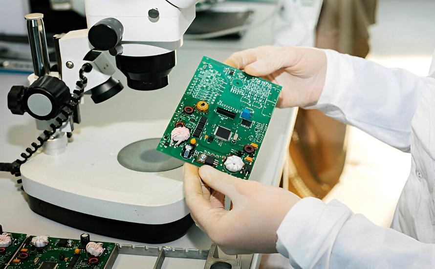
Quality Control in Telecom PCB Assembly
Quality assurance is a critical aspect of telecom PCB assembly because communication systems demand exceptional reliability. Manufacturers employ multiple inspection and testing methods throughout production to ensure compliance with industry standards.
Automated Optical Inspection systems verify component placement, solder joint quality, and assembly accuracy. These systems quickly identify manufacturing defects that could affect performance.
X-ray inspection is commonly used for advanced semiconductor packages with hidden solder connections. This technology provides detailed visibility into internal solder joints and helps detect defects that may not be visible externally.
Electrical testing procedures such as In-Circuit Testing and functional testing verify circuit performance and ensure that the assembly operates according to specifications.
Environmental and reliability testing may also be conducted to evaluate product durability under real-world operating conditions.
Telecom PCB Assembly and 5G Technology
The rollout of 5G networks has significantly increased demand for advanced telecom PCB assembly solutions. 5G infrastructure requires highly sophisticated electronic systems capable of supporting faster data speeds, lower latency, and greater network capacity.
These requirements have driven the adoption of high-frequency materials, advanced multilayer PCB designs, and precision assembly processes. Telecom manufacturers must produce assemblies that support millimeter-wave frequencies and complex signal-processing functions.
The growth of 5G technology is expected to continue driving innovation in PCB manufacturing and assembly techniques, creating new opportunities for advanced telecommunications products.
As network infrastructure evolves, telecom PCB assembly will remain a fundamental component of communication technology development.
The Future of Telecom PCB Assembly
The future of telecom PCB assembly is closely linked to ongoing advancements in communication technologies. Emerging applications such as 6G research, edge computing, artificial intelligence, cloud networking, and IoT connectivity will require increasingly sophisticated electronic hardware.
Manufacturers are investing in advanced automation systems, intelligent inspection technologies, and smart manufacturing processes to improve production efficiency and quality. High-density interconnect boards, embedded components, and next-generation materials are also expanding the capabilities of telecom electronics.
As global demand for connectivity continues to rise, telecom PCB assembly will play an increasingly important role in supporting faster, more reliable, and more intelligent communication networks.
Conclusion
Telecom PCB assembly is a vital manufacturing process that enables the reliable operation of modern communication systems. From cellular networks and fiber-optic infrastructure to routers, switches, satellite equipment, and emerging 5G technologies, telecom PCBs support the transmission and management of vast amounts of data across the globe. Through advanced manufacturing techniques, precise component placement, rigorous quality control, and innovative design practices, telecom assemblies deliver the performance and reliability required by today’s communication networks. As telecommunications technology continues to evolve, businesses increasingly depend on an experienced telecom PCB assembly service provider to ensure high-quality production, dependable performance, and scalable manufacturing solutions for next-generation communication equipment.